A private laboratory specialized in the analysis, testing and failure analysis of materials since 1993
A private laboratory specialized in the analysis, testing and failure analysis of materials since 1993
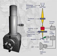
This equipment can quickly provide information on the morphology and elemental composition of a solid object. Its great ease of use, flexibility for viewing highly variable extension fields on massive samples, and the extent of its depth of field make SEM a vital tool in the exploration of the microscopic world.
It consists of two coupled devices:
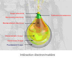
![]() The SEM : an electron microscopy technique based on the principle of electron-matter interactions, capable of producing high resolution images of the surface of a sample.
The SEM : an electron microscopy technique based on the principle of electron-matter interactions, capable of producing high resolution images of the surface of a sample.
![]() The EDS microanalysis : the EDS detector receives photons emitted by the material due to electronic excitation, and sorts them according to their energy. Each energy value being characteristic of the energy level of a chemical element, it is possible to identify the elements contained in the material.
The EDS microanalysis : the EDS detector receives photons emitted by the material due to electronic excitation, and sorts them according to their energy. Each energy value being characteristic of the energy level of a chemical element, it is possible to identify the elements contained in the material.
This technique provides information that is simultaneously morphological (images) and chemical (elemental composition) of a sample.


Apparatus :
HITACHI S3000N, S3400N, SU3500 Variable Pressure Scanning Electronic Microscope :
![]() Magnification up to x100,000
Magnification up to x100,000
![]() Variable pressure -> No metallization on non-conductive samples
Variable pressure -> No metallization on non-conductive samples
![]() Peltier plate: freezing of organic samples at -30 ° C for non-destructive observation
Peltier plate: freezing of organic samples at -30 ° C for non-destructive observation
![]() Two image types: topographic contrast (SE mode)
Two image types: topographic contrast (SE mode)
![]() chemical contrast (BSE mode)
chemical contrast (BSE mode)
EDX detector UltraDry, Thermo Electron :
![]() Si Crystal, NORVAR window
Si Crystal, NORVAR window
![]() Detection from beryllium
Detection from beryllium
![]() Energy resolution: 132 eV on the K ray (Mn)
Energy resolution: 132 eV on the K ray (Mn)
![]() Spatial resolution: 1 µm3
Spatial resolution: 1 µm3